Logic Circuit Diagram Of 1 To 8 - 3 Logic Circuits Boolean Algebra And Truth Tables Dr Stienecker S Site - From a modeling perspective, this.. [aj block diagram and b circuit. Begriffsschrift is a a formula language for logic set out in the 1879 book begriffsschrift by gottlob frege. Boolean expression we will discuss each herein and demonstrate ways to convert between them. Draw the circuit diagram of the sequence detector. The circuit has 3 inputs and 8 outputs design a verilog module for a 3 to 8 decoder using behavior modeling.
A majority gate is a digital circuit whose output is equal to 1 if majority of its inputs. Contemporary computer aided design and analysis software is used throughout. Ee 260l lab 7 b37c 1 to 8 demultiplexer logic diagram wiring resources. We can consider them in many respects to be purely a logic circuit, with an effectively instantaneous output change that reflects the change in inputs. A circuit diagram (electrical diagram, elementary diagram, electronic schematic) is a graphical representation of an electrical circuit.
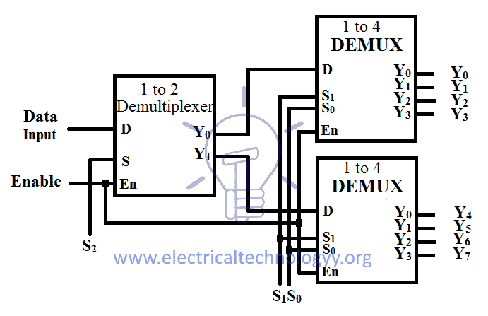
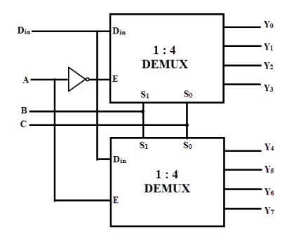
Demux Demultiplexer Types Construction Applications from www.electricaltechnology.org The list of all possible inputs are arranged in columns on. The logical circuit of this ram is shown in figure (13). Design of asynchronous circuits, synchronous sequential circuits, and finite state machines, is covered. The output at any given time depends completely upon the circuit there may be additional logic circuitry to select between the different outputs. Karnaugh mapping techniques and state tables and diagrams are taught. It is also called as 3 to 8 demux because of the 3 selection lines. Cfbab multiplexer logic diagram and truth table digital resources. Let the input be d, s1 and s2 are two select lines and eight outputs from y0 to y7.
The output at any given time depends completely upon the circuit there may be additional logic circuitry to select between the different outputs.
Complete the timing diagram (note that. Led flasher circuit diagram with luxeon v star led. Design of asynchronous circuits, synchronous sequential circuits, and finite state machines, is covered. Karnaugh mapping techniques and state tables and diagrams are taught. Circuit diagram is a free application for making electronic circuit diagrams and exporting them as images. Create a logic diagram of the schematic design entry for a 3 to 8 decoder. Solved combinational logic eircuits are the circuits whos. It is also called as 3 to 8 demux because of the 3 selection lines. When the binary input is 0, 1, 2, or 3, the binary output is one greater than the input. In practice many logic circuits are built using only nand and nor gates because the basic gates in some of the logic families such as ttl and cmos are nand and nor 106 chapter four implementation of logic functions. — an algebraic expression for a boolean function ⇒ a ckt diagram composed of logic gates. The circuit diagram of 4x1 multiplexer is shown in the following figure. Ee 260l lab 7 b37c 1 to 8 demultiplexer logic diagram wiring resources.
A schematic diagram comprises one or more circuit components, interconnected by wires. 1 to 8 demultiplexer logic diagram. How to implement a 1 64 demux using a 1 16 and a 1 4 demux. Transcribed image text from this question. In logic circuit design, this condition should be avoided by making sure that 1's are not applied to both inputs simultaneously.
How To Implement 4 To 1 Mux Using A Decoder Quora from qph.fs.quoracdn.net A majority gate is a digital circuit whose output is equal to 1 if majority of its inputs. The logic diagram of the 3 to 8 line decoder is shown below. Design of asynchronous circuits, synchronous sequential circuits, and finite state machines, is covered. Triac dimmable led driver 14 w circuit diagram. Clap switch circuit clap on circuit diagram हिंदी में पड़ें in this post, i will tell you how to make a clap switch circuit. Here is an implementation using four nand gates originally answered: Browse circuits made by other users of circuit diagram. Draw the circuit diagram of the sequence detector.
The logic diagram of the 3 to 8 line decoder is shown below.
· apply various input data to the logic circuit via the input logic switches. It is also called as 3 to 8 demux because of the 3 selection lines. Block diagram of 1 to 8 demultiplexer. Vhdl code for 1 to 4 demux. From a modeling perspective, this. Design of asynchronous circuits, synchronous sequential circuits, and finite state machines, is covered. Similarly, you can implement 8x1 multiplexer and 16x1 multiplexer by following the same procedure. Contemporary computer aided design and analysis software is used throughout. It is the reverse process of an encoder. A demultiplexer is a combinational logic circuit that receives information on a single line and transmits this information on one of 2 n possible output in 1 to 8 demultiplexer, 1 represents demultiplexer input and 8 represents the number of output lines. Mux working symbol and logic diagram. Browse circuits made by other users of circuit diagram. The outputs of combinational logic circuits are only determined by the logical function of their current input state, logic 0 or logic 1, at any given.
This is called a majority logic circuit. Cfbab multiplexer logic diagram and truth table digital resources. Create a logic diagram of the schematic design entry for a 3 to 8 decoder. The list of all possible inputs are arranged in columns on. Circuit diagram is a free application for making electronic circuit diagrams and exporting them as images.
What Is Demultiplexer Different Types Of Demultiplexers from www.elprocus.com This is great to create complex logic circuits and can be easily be made into a subcircuit. Block diagram of 1 to 8 demultiplexer. The output of the sr latch is simply the state so is not shown separately on this state diagram. Logic diagrams are diagrams in the field of logic, used for representation and to carry out certain types of reasoning. Let the input be d, s1 and s2 are two select lines and eight outputs from y0 to y7. Demultiplexer and 1 to 2 demultiplexer, combinational circuit in digital electronics, #demultiplexer. Combinational logic circuits can be classified as digital logic circuits that do not have any storage elements. 1 to 8 demultiplexer logic diagrams may be categorized in line with use or intent, as an example, explanatory and/or how to 1 to 8 demultiplexer.
Clap switch circuit clap on circuit diagram हिंदी में पड़ें in this post, i will tell you how to make a clap switch circuit.
Let the input be d, s1 and s2 are two select lines and eight outputs from y0 to y7. From simple gates to complex sequential circuits, plot timing diagrams, automatic circuit generation, explore automatically generate circuit based on truth table data. A demultiplexer is a combinational logic circuit that receives information on a single line and transmits this information on one of 2 n possible output in 1 to 8 demultiplexer, 1 represents demultiplexer input and 8 represents the number of output lines. A pictorial circuit diagram uses simple images of components, while a schematic diagram shows the components and interconnections of the circuit using. Similarly, you can implement 8x1 multiplexer and 16x1 multiplexer by following the same procedure. We can easily understand the operation of the above circuit. Cfbab multiplexer logic diagram and truth table digital resources. Design a combinational circuit with three inputs, x, y and z, and the three outputs, a, b, and c. In practice many logic circuits are built using only nand and nor gates because the basic gates in some of the logic families such as ttl and cmos are nand and nor 106 chapter four implementation of logic functions. The circuit diagram of 4x1 multiplexer is shown in the following figure. — an algebraic expression for a boolean function ⇒ a ckt diagram composed of logic gates. Circuit diagram is a free application for making electronic circuit diagrams and exporting them as images. Draw the circuit diagram of the sequence detector.